

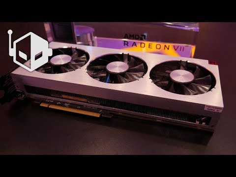
With only a week away from its launch the AMD Radeon VII 7nm GPU appears to have made it’s way to reviewers hands. When the Radeon VII launches next Thursday (2/7/2019) it will become the worlds first 7nm gaming focused GPU. Having taken the Vega architecture and shrunk things down from 14nm to 7nm gave the team at Radeon to find an interesting way to spend the new power envelope they have to work with, and according to their marketing speed is where they put their bet. Reducing the compute unit count down from the 64 that the RX Vega 64 enjoyed down to 60 shouldn’t put any damper on performance with the new target clock rate sitting pretty at 1800MHz. Memory is where another dose of magic gets dropped as we see a doubling of memory capacity and memory bandwidth with 16GB of HBM2 rocking a very wide 1TB/s of memory bandwidth, should prove more than useful at higher resolutions.
But, we’ve seen the card at CES and we’ve seen the renders floating around, but it appears that Legit Reviews and TweakTown are confirmed to have the card in hand. Anthony at TweakTown took it a step further with a shot of it on his test bench while Nathan simply mentioned that they were already underway with testing at Legit Reviews.
Embargo Break?
It has been brought to my attention that there is an ‘unboxing’ embargo for Radeon VII. I don’t have access to that information since I have not been extended an embargo on the Radeon VII or else this article wouldn’t even exist. But, I guess technically neither of these posts are an ‘unboxing’ but rather the card itself, interesting way to skirt around that one.
Currently benchmarking and working on Radeon VII content. Can’t wait to show you what @AMDGaming and @Radeon has been working on.
First 7nm GPU
16GB of HBM2
Launching Feb 7th for $699#RadeonVII #PCGaming #amd #radeon pic.twitter.com/yvxqLYIlN7— Nathan Kirsch (@LegitReviews) February 1, 2019
Radeon VII being tested. World’s first 7nm gaming GPU + 16GB HBM2 @ 1TB/sec. Will there be a big improvement? Are the leaks of RTX 2080 level performance true? You won’t have much longer to find out. Is there something specific you want to see tested? I’ve got 8K benchmarkin… pic.twitter.com/gqygZGcs4Z
— TweakTown (@TweakTown) February 1, 2019
Early 3DMark Leaks
Of course we’ve already seen a few leaked numbers coming from the 3DMark database thanks to the purveyor of leaks, Tum Apisak on twitter. This gave us a bit of an insight on what to expect performance wise, at least in the 3DMark suite. AMD proposed on stage that this card would be posed to take on the GeForce RTX 2080 in recent titles going so far as to show some results on stage at CES. This prompted a bit of a rebuttal from a less than impressed NVIDIA CEO Jensen Huang. We’ve included the benchmarks from the video below for those who don’t feel inclined to watch it.


AMD Radeon Vega VII Specs Comparison:
| Graphics Card | AMD Radeon R9 Fury X | AMD Radeon Vega 64 | AMD Radeon Vega VII |
|---|---|---|---|
| GPU | Fiji XT | Vega 10 | Vega 20 |
| Process Node | 28nm | 14nm | 7nm |
| Compute Units | 64 | 64 | 60 |
| Stream Processors | 4096 | 4096 | 3840 |
| Raster Operators | 64 | 64 | 64 |
| Texture Mapping Units | 256 | 256 | 240 |
| Clock Speed (Peak) | 1050 MHz | 1677 MHz (Liquid) | 1800 MHz |
| FP32 Compute | 8.6 TFLOPs | 13.7 TFLOPs (Liquid) | 13.8 TFLOPs |
| Memory (VRAM) | 4 GB HBM | 8 GB HBM2 | 16 GB HBM2 |
| Memory Bus | 4096-bit | 2048-bit | 4096-bit |
| Memory Bandwidth | 512 GB/s | 484 GB/s | 1 TB/s |
| TDP | 275W | 350W (Liquid) | 300W |
| Power | Dual 8 Pin | Dual 8 Pin | Dual 8 Pin |
| Price | $649 US | $699 US (Liquid) | $699 US |
| Launch | 2015 | 2017 | 2019 |
The post AMD Radeon VII 7nm GPU Makes Its Way To Reviewers Test Benches appeared first on Wccftech.