
The design of most leading edge processors and ASICs rely on steps of optimization, with the three key optimization points being Performance, Power, and Area (and sometimes Cost). Once the architecture of a chip is planned, it comes down to designing the silicon of that chip for a given process node technology, however there are many different ways to lay the design out. Normally this can take a team of engineers several months, even with algorithmic tools and simulation to get a good result, however that role is gradually being taken over with Machine Learning methods. Cadence today is announcing its new Cerebrus integrated ML design tool to assist with PPA optimization – production level silicon is already being made with key partners as the tool directly integrates into Cadence workflows.
Place and Route: The Next Stage of Automation
The act of finding the best layout for a chip, or even for a part of a chip such as a macro or a library, has already been optimized for many years – engineers plug in details about the parts of the design with a variety of parameters and run overnight simulations to find the best layout. These algorithmic implementations of ‘Place and Route’ have been built over time to be very complex, but rely on equations and if/then statements to try and predict the best design. Very often this is a slow process, with the engineering team having to go back, tweak the design, and attempt again. The designs are then simulated for expected performance and power to find which is the best. There is no level of the software ‘learning’, as the algorithm is defined by hard and fast rules.
The advancement of machine learning this decade has put a new twist on traditional Place and Route algorithms. Companies that build EDA (Electronic Design Automation) tools to design chips have been researching into the best way to integrate machine learning into their algorithms with the hope that the software alone can understand what it is doing, make iterative improvements, and essentially be left to its own devices to get the best result. Beyond this, it allows for parallel analysis across many systems – one of the main limitations of traditional EDA test and simulation is that it is single thread limited and doesn’t scale, whereas ML would allow for more parallel testing and simulation.
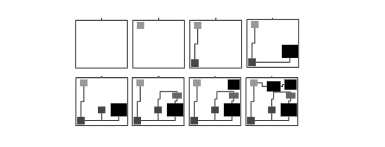
An example of ML-assisted design from Google
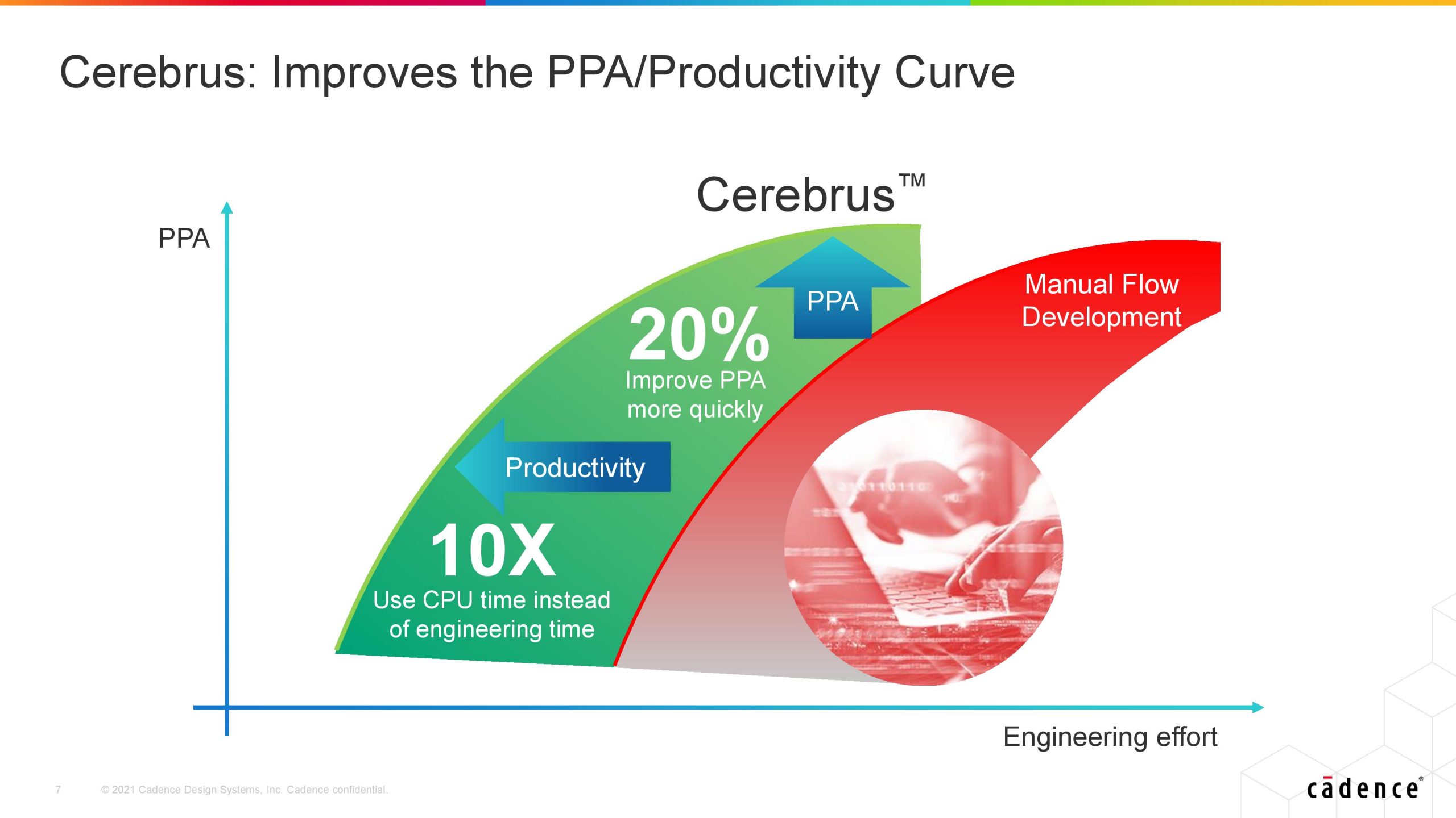
In speaking to EDA companies that are discussing ML tools, the main benefit of this technology is that it creates a simpler workflow but also produces better processors almost equivalent to a benefit of a whole process node. What would take a team of a dozen engineers half a year to find a good design can be superseded by one or two engineers over a couple of weeks, and it would end up with a better PPA than the human plus non-ML methods ever could.
How To Enable Machine Learning on EDA
Today’s announcement is from Cadence, one of the top EDA tool vendors, with the launch of their new Cerebrus technology. Integrated directly into the Cadence toolchain, Cerebrus can work at any level of the stack design, from high level definitions in System C down to standard cells, macros, RTL and signoff, and it allows an engineer to give it objects with defined specifications at any level and optimize for each. The automated floorplanning allows for the engineer to specify optimization points beyond regular PPA, such as wire length, wire delay, power grid distribution, IR drop, IO placement with respect to physical chip boundaries, and other parameters.
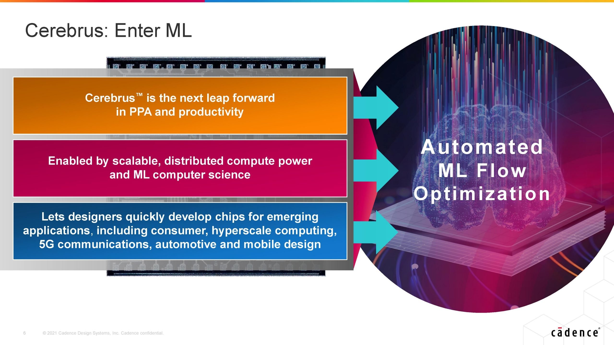
Cadence’s Cerebrus tool uses reinforcement machine learning for its optimization process – the technology is already in hands with key customers and in use with chip design, although today’s announcement makes it available to the wider customer base. Cadence states that the machine learning workflow is designed such that it can start from an untrained model and find an optimized point in 50-200 iterations, and within an organization models can be reused if a number of constraints are followed (process node PDK, similar structure) reducing that time even further. Theoretically an organization can build a library of pre-trained models, and enable Cerebrus to attempt the best one for the task, and if that fails, start anew and still get a great result.
One of the common questions I ask about these new advancements is how well the end design can be fed back to engineers to help with higher level design – it is all very well the ML portion of the tool working on reinforcement learning, but is there anything that can be done to assist the engineer in their understanding of their own architectural implementation. In speaking with Cadence’s Kam Kittrell, he explained that a key value of their tool is a replay feature – it records each iteration in the reinforcement learning process, allowing engineers to step through how each cycle decided to do what it did, allowing the engineer to understand why the end result the way it is. I haven’t heard of any other EDA company having this feature at this time.
Cadence Cerebrus Case Studies
As part of the announcement today, two of Cadence’s partners contributed quotes to the efficacy of the technology, however it is the case studies provided that are worth looking over.
First up is a 5nm mobile CPU, which we believe to be part of Cadence’s partnership with Samsung Foundry. According to the information, the Cerebrus tool helped a single engineer in 10 days achieve a 3.5 GHz mobile CPU while also saving leakage power, total power, and improving transistor density. Compared to a predicted timeline using almost a dozen engineers over several months, it is predicted that Cerebrus improved the best hand tuned design for a +420 MHz frequency gain, saving 26 mW of leakage power and 62 mW of total power.
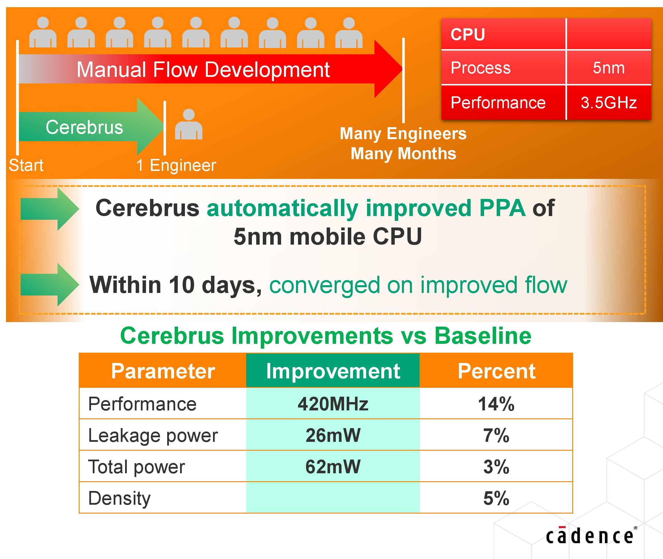
62 mW of total power, as a 3% saving, suggests a 2 W chip (or core). Right now Samsung does not have a 3.5 GHz 5nm mobile processor in the market, but it does suggest that future designs will be more optimized than before.
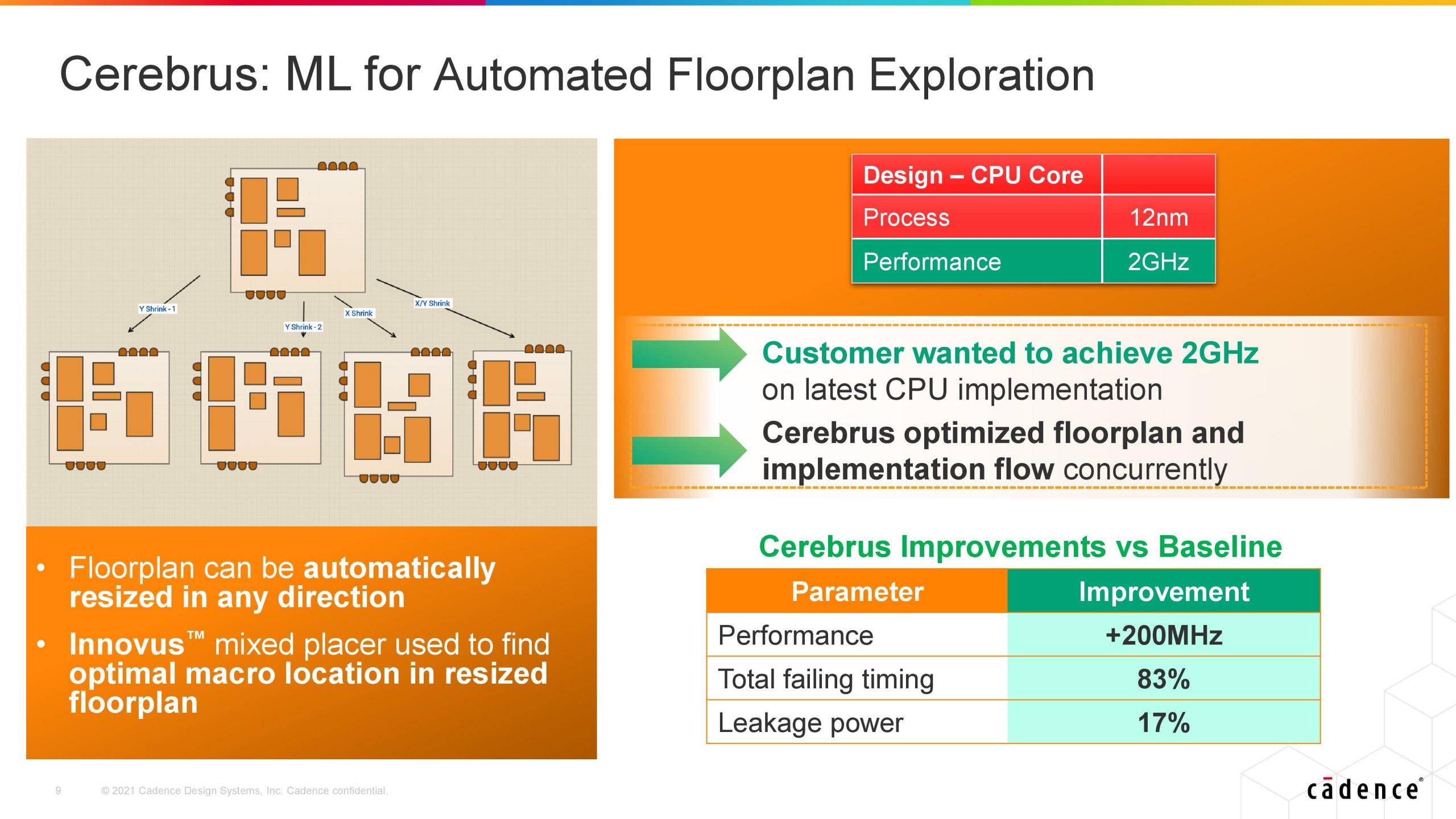
The second case study involves floorplan optimization and implementation optimization concurrently. In this instance Cadence says a customer wanted a 12nm CPU core at 2 GHz with the lowest power and lowest area, and the Cerebrus tool was able to optimize for that 2 GHz point, reducing wire delay timing by 83% as well as leakage power by 17%.
Samsung Foundry is already rolling out Cerebrus as part of its DTCO program for partners that have a Cadence based workflow.
The Future of ML-enhanced EDA Tools
We recently reported a similar story from the other heavyweight in the EDA industry, Synopsys, about its DSO.ai software. Synopsys has a keynote titled ‘‘Does Artificial Intelligence Require Artificial Architects?’ at this year’s Hot Chips conference, where we expect to hear more information about the work they’re doing with customers. In a similar light, we expect Cadence to also discuss more about wins with its Cerebrus tools.
However, a question I put both companies is about the evolution of the software. There are ultimately two roadmaps for software like DSO.ai and Cerebrus – function and performance. To a certain extent it’s easy to talk about a roadmap of function as the companies’ research and enable ML tools to work across more of the toolchain (as well as potentially violating standard abstraction layer boundaries). But the performance is a big question – while scaling out performance with more tests is ‘easy’ to build for, developing relative ML algorithms that are easier to find the best layouts is going to be a very wide field to discover. Floorplanning designs have millions of degrees of freedom to optimize for, and one of the limitations of human involvement is getting stuck going down one particular design route; with so much to explore, neither company yet is discussing what their plans are to ensure that ML-assisted design can overcome these potential obstacles. Most likely, as the technology becomes more widely adopted, exactly how that development with coalesce into actual research and product roadmaps might become something more tangible for a roadmap of sorts.