
We’re gearing up for a busy time when it comes to server announcements, with the recent news that AMD will be launching its next generation platform on March 15th, but also we are expecting Intel to disclose its Ice Lake Xeon Scalable platform sometime soon as well. To that point, in an on-the-record discussion I had today, Intel disclosed some interesting numbers about the state of Ice Lake Xeon Scalable deployment.
The usual fare when it comes to enterprise processor launches is that the key customers have already had the hardware in hand for at least three to six months, if not more. These key customers, usually hyperscalers, pay in advance for thousands of units to help deploy their infrastructure. They use the hardware to optimize their code, but also help the processor manufacturer test for bugs in early silicon, and then build out their infrastructure when it’s ready. This has been the way for server processor deployments for over a decade or two, and for the upcoming launches, both AMD and Intel have disclosed that they’ve been in high-volume manufacturing of their latest products for some time now, with key customer deployments already taking place.
Finding numbers for how big these deployments prior to launch is often tricky. Even the order of magnitude is somewhat hard to decipher – these companies could be deploying hundreds, thousands, perhaps millions of processors well before the official public launch. A lot of it comes down to production availability, and optimizing for the customers that matter most first, before moving out to the main launch and general availability.
So cue my surprise that today, in an on-the-record call with Intel SVP and GM of the Xeon Memory Group Lisa Spelman, as we were discussing Intel’s enterprise strategy as it relates to offering complete solutions, open source libraries, and automatic optimizations on the latest feature set, some numbers were given. Lisa stated that, to date, Intel has shipped 115,000 units of Ice Lake Xeon Scalable to 30 of its key advance customers.
It’s hard to gauge what sort of time frame these deployments were made over – Intel has recently stated that through 2020 it was able to double its silicon production capacity, with its 10nm product lines getting the best percentage boost in that metric. However, Intel originally stated that it was sampling Ice Lake Xeon with key customers as far back as May 2019. With high volume manufacturing starting in Q4 and into Q1, there is obviously an ecosystem and supply chain inside Intel designed to churn out working silicon and put it into the hands of customers. It’s hard to decipher if this 115,000 number is better or worse than previous launches, due to lack of data, however it is a substantial amount of silicon to ship in advance of a full launch and wider general availability.

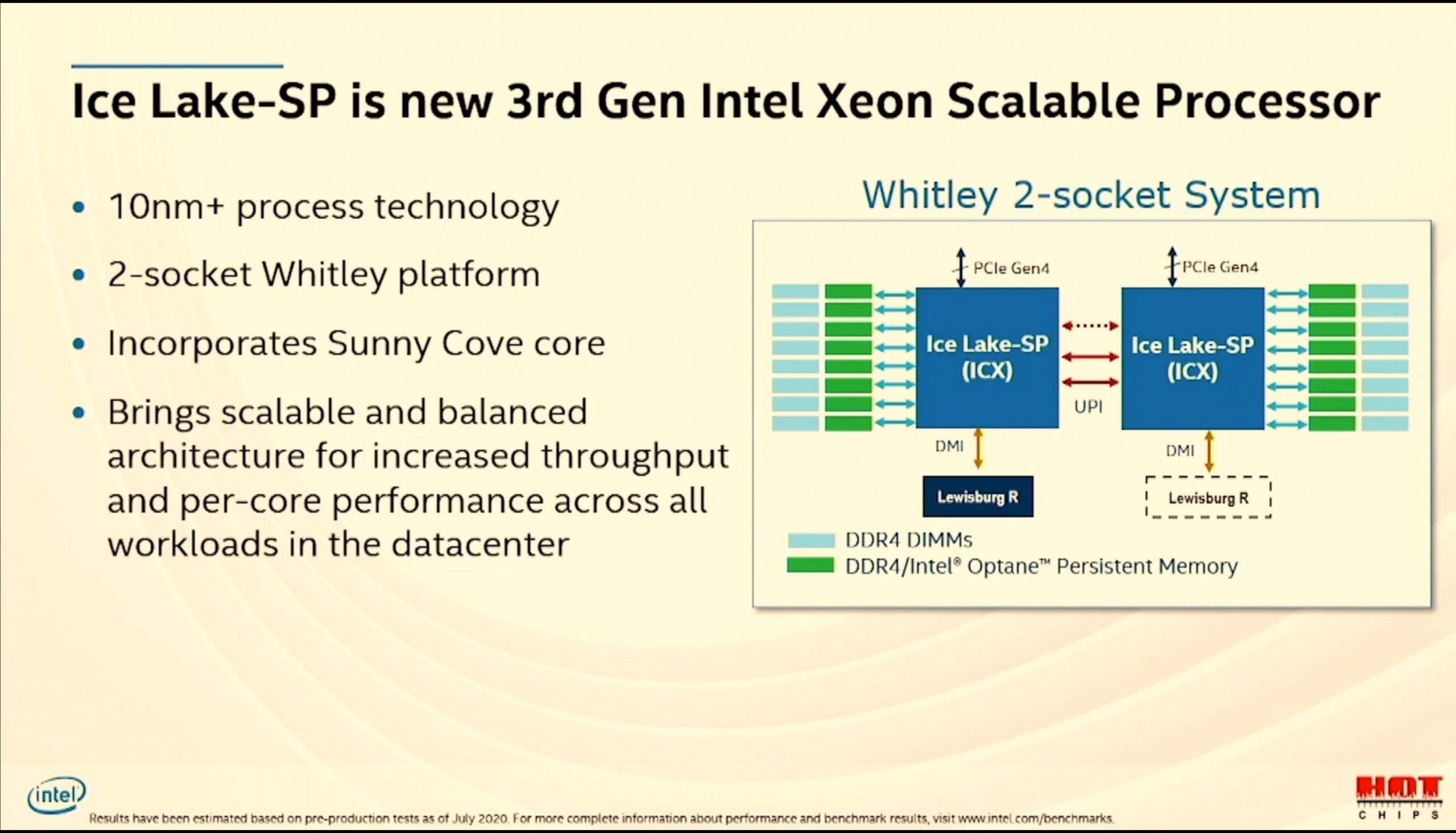
Lisa also stated that enabling their ecosystem with full stack solutions, building on raw performance with optimized codebases, is going to be a critical part of Intel’s strategy as it rolls out Ice Lake and future generations of Intel Xeon Scalable, alongside Intel’s other adjacent product lines (FPGA, networking, Optane DCPMM, SSD, AI accelerators). This means that alongside discussing generational updates of the key components, the discussion is also fundamentally driven by the platform as the sum of its parts.
There was also mention of the desire to enable a regular expected cadence of underlying performance improvements generation on generation, coupled with tools to accelerate customer workload that are easier to use and open source. This is being enabled as a core part of how Intel’s enterprise divisions have been architected over 2020. That includes enabling the wider ecosystem outside Intel with optimizations that used to be under Intel license, as well as pooling updated improvements for other open source solutions with the community.

Intel hasn’t formally disclosed a launch date for its upcoming Xeon Scalable 3rd Generation Ice Lake processor family, simply stating in January that it will be ‘in the coming months’. When it does, be sure to read about all the fine details here at AnandTech.
Update: Just some back of the napkin math here. Intel’s middle die-size HCC on Skylake Xeon Scalable was ~480 mm2, with a production rate of 108 per wafer, assuming perfect yield. Let’s work on the assumption that this would be a good die size for Ice Lake Xeon (more cores, denser 10nm process). If Intel’s defect rate for 10nm was as good as TSMC’s N7, for which we know the latter to be a rate of 0.09 defects per cm2, the actual yield would be 71 dies per wafer, which equates to 66%. If Intel was extracting 71 dies per wafer, then 115,000 dies would be around 1620 wafers. We don’t know at this point if Intel is absorbing some of those defects by having more physical cores on the die than will be offered, and this doesn’t take into account reduced die count configurations (e.g. a 20 core part from a 28-core die). But it’s an interesting number.