
This article is part of the Technology Insight series, made possible with funding from Intel.
We tend to focus on the latest and greatest technology nodes because they’re used to manufacture the densest, fastest, most power-efficient processors. But as we were reminded during Intel’s recent Architecture Day 2020, a range of transistor designs is needed to build heterogeneous systems.
“No single transistor is optimal across all design points,” said chief architect Raja Koduri. “The transistor we need for a performance desktop CPU, to hit super-high frequencies, is very different from the transistor we need for high-performance integrated GPUs.”
Here’s the problem: gathering processing cores, fixed-function accelerators, graphics resources, and I/O, and then etching them all onto a monolithic die at 10nm makes manufacturing very, very, difficult. But the alternative—breaking them apart and linking the pieces—presents challenges of its own. Innovations in packaging overcome these hurdles by improving the interface between dense circuits and the boards they populate.

Above: Advanced packaging is all about mixing and matching the right transistors for each application to speed time to market while maximizing performance.
Image Credit: Intel
Back in 2018, Intel laid out a plan to get smaller devices working together without sacrificing speed. “We said that we need to develop technology to connect chips and chiplets in a package that can match the performance, power efficiency, and cost of a monolithic SoC,” continued Koduri. “We also said we need a high-density interconnect roadmap that enables high bandwidth at low power.”
In an industry eager to name winners and losers based on process technology, innovative approaches to packaging will be force multipliers in the battle for computing supremacy. Let’s look at Intel’s current packaging playbook, along with the teasers disclosed during its recent Architecture Day 2020.
KEY POINTS:
- The Embedded Multi-die Interconnect Bridge (EMIB) facilitates die-to-die connections using tiny silicon bridges embedded in the package substrate
- The Advanced Interface Bus (AIB) is an open-source interconnect standard for creating high-bandwidth/low-power connections between chiplets
- Foveros takes packaging to the third dimension with stacked dies. The first Foveros-based product will target the space between laptops and smartphones.
- Co-EMIB and the Omni-Directional Interface promise scaling beyond Intel’s existing packaging technologies by facilitating greater flexibility.
Overcoming monolithic growing pains with EMIB
Until recently, if you wanted to get heterogeneous dies onto a single package for maximum performance, you placed those dies on a piece of silicon called an interposer and ran wires through the interposer for communication. Through silicon vias (TSVs) — electrical connections — passed through the interposer and into a substrate, which formed the package’s base.
The industry refers to this as 2.5D packaging. TSMC used it to manufacture NVIDIA’s Tesla P100 accelerator back in 2016. A year before that, AMD combined a massive GPU and 4GB of high-bandwidth memory (HBM) on a silicon interposer to create the Radeon R9 Fury X. Clearly, the technology works. But it adds an inherent layer of complexity, cutting into yields and adding significant cost.
Intel’s Embedded Multi-die Interconnect Bridge (EMIB) aims to mitigate the limitations of 2.5D packaging by ditching the interposer in favor of tiny silicon bridges embedded in the substrate layer. The bridges are loaded with micro-bumps that facilitate die-to-die connections.
“The current generation of EMIB offers a 55 micron micro-bump pitch with a roadmap to get to 36 microns,” said Ramune Nagisetty, director of process and product integration at Intel. Compare that to the 100-micron bump pitch of a typical organic package. EMIB makes it possible to achieve much higher bump density as a result.
Small silicon bridges are also a lot less expensive than interposers. Whereas the Tesla P100 and Radeon R9 Fury X were high-dollar flagships, one of Intel’s first products with embedded bridges was Kaby Lake G, a mobile platform that combined eighth-gen Core CPUs and AMD Radeon RX Vega M graphics. Laptops based on Kaby Lake G weren’t cheap by any measure. But they demonstrated EMIB’s ability to get heterogeneous dies onto one package, consolidating valuable board space, augmenting performance, and driving down cost compared to discrete components.
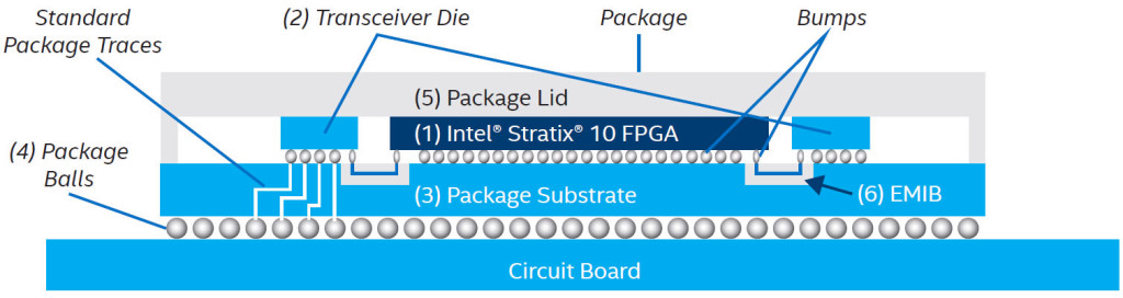
Above: In this example, EMIB creates a high-density connection between the Stratix 10 FPGA and two transceiver dies.
Image Credit: Intel
Intel’s Stratix 10 FPGAs also employ EMIB to connect I/O chiplets and HBM from three different foundries, manufactured using six different technology nodes, on one package. By decoupling transceivers, I/O, and memory from the core fabric, Intel can pick and choose the transistor design for each die. Adding support for CXL, faster transceivers, or Ethernet is as easy as swapping out those modular tiles connected via EMIB.
Standardizing die to die integration with the Advanced Interface Bus
Before chiplets can be mixed and matched, the reusable IP blocks must know how to talk to each other over a standardized interface. For its Stratix 10 FPGAs, Intel’s embedded bridges carry the Advanced Interface Bus (AIB) between its core fabric and each tile.
AIB was designed to enable modular integration on a package in much the same way PCI Express facilitates integration on a motherboard. But whereas PCIe drives very high speeds through few wires, AIB exploits the density of EMIB to create a wide parallel interface that operates at lower clock rates, simplifying the circuitry to transmit and receive while still achieving very low latency.

Above: Reusable IP blocks on a package may be connected by silicon bridges or interposers using the Advanced Interface Bus to move data over a wide parallel connection.
Image Credit: Intel
The first generation of AIB offers 2 Gb/s wire signaling, enabling Intel’s vision of heterogeneous integration with monolithic SoC-like performance. A second-generation version, expected to tape out in 2021, supports up to 6.4 Gb/s per wire, bump pitches as tight as 36 microns, lower power per bit transferred, and backward compatibility with existing AIB implementations.
It’s worth noting that AIB is packaging agnostic. Although Intel connects its tiles using EMIB, TSMC’s Chip-on-Wafer-on-Substrate (CoWoS) technology could carry AIB, too.
Earlier this year, Intel became a member of the Common Hardware for Interfaces, Processors, and Systems (CHIPS) Alliance, hosted by the Linux Foundation, to contribute the AIB license as an open-source standard. The idea, of course, was to encourage industry adoption and facilitate a library of AIB-equipped chiplets.
“We currently have 10 AIB-based tiles from multiple vendors that are either in-production or on power-on,” says Intel’s Nagisetty. “There are 10 more tiles in the near-term horizon from ecosystem partners including startups and university research groups.”
Foveros increases density in a third dimension
Breaking SoCs into reusable IP blocks and integrating them horizontally with high-density bridges is one of the ways Intel plans to leverage manufacturing efficiencies and continue scaling performance. The next step up, according to the company’s packaging technology roadmap, involves stacking dies on top of each other, face-to-face, using fine-pitched micro-bumps. This three-dimensional approach, which Intel calls Foveros, closes the distance between dies, using less power to move data around. Whereas Intel’s EMIB technology is rated at roughly 0.50 pJ/bit, Foveros gets that down to 0.15 pJ/bit.
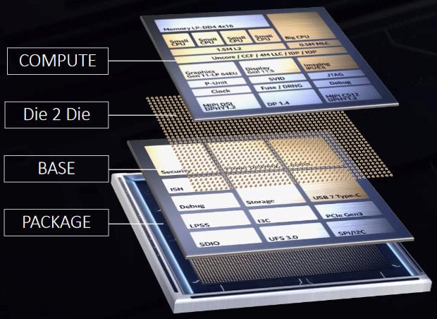
Above: Lakefield, the first product based on Foveros 3D die stacking, comprises a base die (22FFL) under a compute die (10nm), all of which is topped by package-on-package memory.
Image Credit: Intel
Like EMIB, Foveros allows Intel to pick the best process technology for each layer of its stack. The first implementation of Foveros, code-named Lakefield, crams processing cores, memory control, and graphics into a die manufactured at 10nm. That chiplet sits on top of the base die, which includes the functions you’d typically find in a platform controller hub (audio, storage, PCIe, etc.), manufactured on a 14nm low-power process. Micro-bumps between the two pipe in power and communications through TSVs in the base die. Intel then tops the stack with LPDDR4X memory from one of its partners.
A complete Lakefield package measures just 12x12x1mm, enabling a new class of devices between laptops and smartphones. But we don’t expect Foveros to only serve low-power applications. In a 2019 HotChips Q&A session, Intel fellow Wilfred Gomes predicted the technology’s future ubiquity. “…the way we designed Foveros, we think it’ll span the entire range of the computing spectrum, from the lowest-end devices to the highest-end devices,” he said.
Scalability gives us another variable to consider
The packaging roadmap set forth during Intel’s Architecture Day 2020 plotted each technology by interconnect density (the number of microbumps per square millimeter) and power efficiency (pJ of energy expended per bit of data transferred). Beyond Foveros, Intel is pursing die-on-wafer hybrid bonding to push both metrics even further. It expects to achieve more than 10,000 bumps/mm² and less than 0.05 pJ/bit.
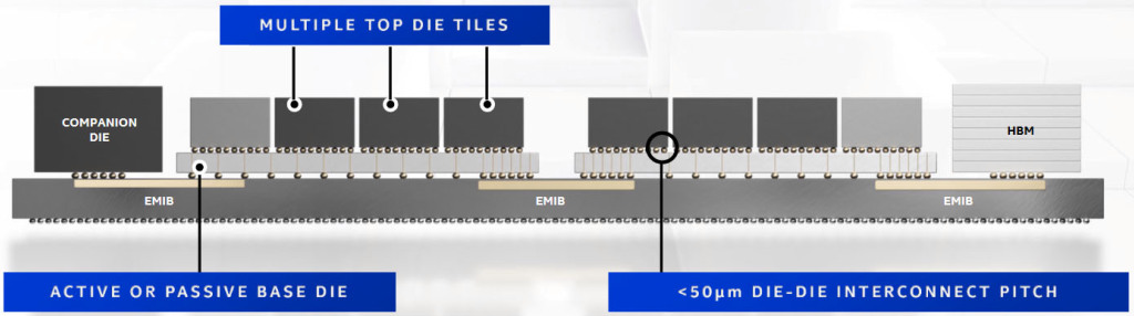
Above: Blending 2.5D and 3D packaging technologies yields Co-EMIB, which enables larger-than-reticle sized base dies plus Foveros die stacks on the same package.
Image Credit: Intel
But advanced packaging technologies can offer utility beyond higher bandwidth and lower power. A combination of EMIB and Foveros — dubbed Co-EMIB — promises scaling opportunities beyond either approach on its own. There are no real-world examples of Co-EMIB yet. However, you can imagine large organic packages with embedded bridges connecting Fovoros stacks that combine accelerators and memory for high-performance computing.
Intel’s Omni-Directional Interface (ODI) offers even more flexibility by linking chiplets next to each other, connecting chiplets stacked vertically, and providing power to the top die in a stack directly through copper pillars. Those pillars are larger than the TSVs that run through the base die in a Foveros stack, minimizing resistance and improving power delivery. The freedom to connect dies in any direction and stack larger tiles on top of smaller ones gives Intel much-needed flexibility in layout. It certainly looks like a promising technology for building on Foveros’ capabilities.