
SK Hynix this week revealed some additional technical details about its upcoming DDR5-6400 memory chip at the International Solid State Circuits Conference. The die size of the company’s 16 Gb DDR5 chip is at a high end of historical DRAM die sizes, so the cost of the device will likely be quite high. However, the increased DRAM density per square millimeter will likely enable SK Hynix to build rather cost effective 8 Gb DDR5 ICs.
The DDR5 memory chip described by SK Hynix is a 16 Gb device (organized in 32 banks and 8 bank groups) that features a 6400 MT/s interface transfer rate at 1.1 Volts. The device is produced using SK Hynix’s second-gen 10nm-class fabrication technology (also known as 1y nm tech) with four metal layers, its die size is 76.22 mm2, reports EETimes.
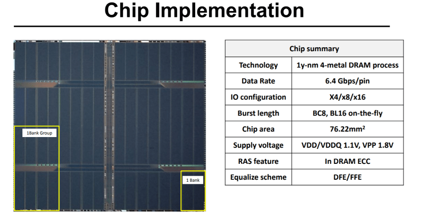
To put the 76.22 mm2 number into context, SK Hynix’s 8 Gb DDR4 DRAM produced using the company’s 1st Gen 21 nm manufacturing process featured a 76mm2 die size, whereas a similar DDR5 device made using the 2nd Gen 21 nm tech had a die size of 53.6 mm2, according to TechInsights. Based on historical die sizes of more or less recent memory devices, a 76mm2 die size may be considered to be rather huge, even though SK Hynix clearly deserves a praise for its DRAM density per square millimeter. In fact, this increased density will enable the company to fabricate relatively low cost 8 Gb DDR5 chips for client PCs.
Apart of higher per-chip capacities compared to DDR4, DDR5 DRAM is set to provide higher performance, which means operation at higher frequencies (read more here). To reduce clock jitter and clock duty cycle distortion that occur because of high frequencies, SK Hynix had to implement a new delay-locked loop (DLL) that uses a phase rotator and an injection locked oscillator. In addition, the chip features a revised forward feedback equalization (FFE) circuit, and a new write-level training method (again, to enable high clocks).

Sources: EETimes, TechInsights